200w Switching Power Supply Protection Scheme. Schemes
Best Scheme of Standard BP ATH
ATX POWER SUPPLY DTK PTP-2038 200W
TL494.
Features:
- Full set of PWM control functions
- Output flowing or flowing current of each exit 200mA
- It is possible to work in a two-stroke or one-step
- Built-in dual pulse suppression scheme
- Wide range adjustment
- Outlet reference voltage 5V + -05%
- Just organized synchronization
general description:
Specially created for the construction of IVP, the TL493 / 4/5 chips provide the developer advanced possibilities when designing IVP control schemes. TL493 / 4/5 devices include an error amplifier, a built-in adjustable generator, a dead-time adjustment comparator, a control trigger, a precision ion by 5V and an output cascade control circuit. The error amplifier issues a simphanist voltage in the range from -0.3 ... (VCC-2) V. The dead time adjustment comparator has a constant displacement that limits the minimum duration of the dead time of the value of about 5%.
It is allowed to synchronize a compared generator, using the connection of R output R to the output of the reference voltage and supply the input sawtooth voltage to the output C, which is used when synchronous operation of several IVP schemes.
Independent outputers on transistors provide the ability to operate the output cascade according to a circuit with a common emitter or by an emitter repeater scheme. The output cascade of the TL493 / 4/5 microcircuit works in one-way or two-stroke mode with the ability to select a mode using a special input. The built-in scheme controls each output and prohibits the issuance of a dual pulse in the two-stroke mode.
The devices having suffix L guarantee normal operation in the temperature range --5 ... 85C, with a suffix with a normal operation in the temperature range of 0 ... 70c.
Structural scheme:

Cocolevka case:

Parameter limit values:
Supply voltage ......................................................................41v
Input voltage amplifier ............................................. ... (VCC + 0.3)
Output voltage collector ................................................ ... ... 41v
Output current collector ........................................................................ ... 250mA
The total dispersion capacity in continuous mode ........................... .1W
Operating range of ambient temperatures:
With suffix L ........................................................................ -25..85С
With a suffix with ........................................................................ ..0..70c
Range of storage temperatures ................................................- 65 ... + 150c
I needed a lightweight power supply, for different cases (expeditions, nutrition of different KV and VHF Trancivers or to move to another apartment not to carry with a transformer BP). After reading the available information on the network, about the alteration of computer BP - I realized that it would be necessary to deal with himself. I found everything, it was described by somehow calm and incomplete (for me). Here I will tell, in order, as I reworked several different blocks. Differences will be described separately. So, I found several BP from the old PC386 with a capacity of 200W (in any case, it was written on the lid). Usually, such as the following are written on the housings of such BP: + 5V / 20A, -5V / 500MA, + 12V / 8A, -12V / 500MA The currents indicated over the tires +5 and + 12V are impulse. It is impossible to constantly load with such currents of BP, high-voltage transistors will also be tested. Take 25% from the maximum pulse current and get the current that the power supply can keep constantly, in this case it is 10a and up to 14-16a briefly (no more than 20s). Actually, it is necessary to clarify that 200W bp is different, there are those who came across not everyone could keep 20a even briefly! Many have dragged only 15a, and some up to 10a. Keep it in mind!

I want to note that the specific model of the BP role does not play, since all of them are made in almost one scheme with small variations. The most critical moment is the presence of the DBL494 chip or its analogues. I came across BP with one microcircuit 494 and with two chips 7500 and 339. Everything else has no importance. If you have the opportunity to choose BP from several, first of all, pay attention to the size of the pulse transformer (the bigger, the better) and the presence of a network filter. Well, when the network filter is already smoky, otherwise it is necessary to penetrate it yourself so that there is no interference. It is easy, wrap 10 turns on the firrite ring and put two capacitors, the places for these parts are already provided on the board.
Priority modifications
To begin with, we will make some simple things, after which you will receive a well-working power supply with an output voltage of 13.8V, direct current up to 4 to 8a and short-term up to 12a. You will make sure that the BP works and decide whethercontinue modifications.
1. We disassemble the power supply and pull out a board from the housing and actively clean it, a brush and a vacuum cleaner. Dust should not be. After that, we drop all the beams of the wires going to the tires +12, -12, +5 and -5v.
2.
You need to find (on the board) DBL494 chip (in other boards costs 7,500, this is analog), switch the priority of protection from the tire + 5V to + 12V and install the voltage you need (13 - 14V).
From the 1st leg of the DBL494 chip departs two resistors (sometimes more, but it's not fundamentally), one goes to the housing, the other to the + 5B bus. He needs us, gently disappear one of his legs (break the connection).
3.
Now, between the tire + 12V and the first knife chip DBL494 we solder a resistor 18 - 33k. You can put a stroke, set the voltage + 14V and then replace it with constant. I recommend setting not 13.8V, namely, on 14.0V, because the majority of the branded KV-VHF equipment works better at this voltage.

Setup and adjustment
1. It's time to turn on our BP to check whether we did everything right. The fan can not be connected and the board itself does not insert into the housing. Turn onboard, without load, to the bus + 12V we connect a voltmeter and see what voltage is there. The trimming resistor, which stands between the first leg of the DBL494 chip and the + 12B china chip, set the voltage from 13.9 to + 14.0V.
2. Now check the voltage between the first and seventh feet of the DBL494 chip, it must be at least 2V and not more than 3B. If this is not the case, pick up the resistor resistance between the first leg and the housing and the first leg and the + 12V tire. Pay special attention to this item, this is a key point. At voltage above or below the specified, the power supply will work worse, unstable, to keep less load.
3. Rock up the thin wire of the tire + 12V on the body, the voltage should be the abyss so that it is restored - turn off the BP for a couple of minutes (It is necessary that the tanks are discharged) And turn on again. Voltage appeared? Okay! As you can see, protection works. What, not worked?! Then throw out this BP, it does not fit and take the other ... hee.
So, the first stage can be considered completed. Insert the board into the case, output the terminals for connecting the radio station. Power supply can be used! Connect the transceiver, but it is impossible to give the load of more than 12a! Automotive VHF station, will work at full power (50W)And in the kV transceiver will have to install 40-60% of power. What will happen if you load the BP with a big current? Nothing terrible, usually triggers protection and disappears the output voltage. If the defense does not work, high-voltage transistors overheat and burst. In this case, the voltage simply disappears and there will be no consequences for the equipment. After their replacement, the BP is operational again!
1. I turn the fan on the contrary, it should pose the housing. Under the two fan screws, put the washers to deploy it slightly, and then blows only on high-voltage transistors, it is incorrectly, it is necessary that the air flow is directed to diode assemblies and on the ferrite ring.
Before that, the fan is preferably lubricated. If it is very noise, put a resistor 60 - 150Ω 2W resistor sequentially with it. Or make a regulator of rotation depending on the heating of the rediators, but about it is slightly lower.
2.
Display two terminals from BP to connect the transceiver. From the 12V bus to the terminal, run 5 wires from that beam which you dropped first. Between terminalsput a non-polar capacitor to 1MKF and a LED with a resistor. Minus wire, also bring five wires to terminal. In some BP, parallel terminals to which the transceiver is connected, put the resistor with a resistance of 300 - 560. This is the load, in order not to have triggered protection. The output chain should look something like that, as shown in the diagram.


two radiator, pulse transformer, choke on a ferrite ring, throttle on a ferrite rod. Now our task is to reduce the heat transfer and increase the maximum load current. As I said earlier, he can reach 16a (for BP power 200W).
4.
Water the throttle on the ferrite rod from the bus + 5V and put it on the + 12V bus, which is previously the choke (It is higher and wound with thin wire) Drop and throw away. Now the throttle to warm up almost will not be or will, but not so much. On some choke charges, it is simply no, you can do without it, but it is desirable that it was for better filtering of possible interference.

5. On a large ferrite ring, throttle to filter pulse interference is wound. The tire + 12V is wound on it with a thinner wire, and the tire + 5 in the most thick. Blow out gently this ring and swap winding places for tires + 12V and + 5V (or turn on all windows parallel). Now the tire + 12V passes through this throttle, the thick wire. As a result, this throttle will heat up significantly less.
6. In BP, two radiator are installed, one for powerful high-voltage transistors, another, for diode assemblies by +5 and + 12V. I came across a few varieties of radiators. If, in your BP, the sizes of both radiators are 55x53x2mm and in the upper part they have edges (as in the photo) - you can count on 15a. When the radiators have a smaller size - it will not be rapidly loaded to load the BP of more than 10a. When the radiators are thicker and have an additional platform at the top - you are lucky, it is the best option, you can get 20a for a minute. If small radiators, to improve heat transfer, can be fixed on them a small plate of duralumin or half from the radiator of the old processor. Please note that high-voltage transients to the radiator are well screwed, sometimes they hang.
7. We drop electrolytic capacitors on the bus + 12V, they put 4700x25V in their place. Capacitors on the + 5B bus are desirable to fall, just to ensure that the places of free more and air blew air from the fan better.


8. On the board you see two high-voltage electrolytes, usually it is 220x200v. Replace them for two 680x350v, in the extreme case, connect parallelly two to 220 + 220 \u003d 440MKF. This is important and the matter is not only in filtration, impulse interference will be weakened and resistance to maximum loads will increase. The result can be found oscilloscope. In general, it must be done!
9. It is desirable that the fan changed the speed depending on the heating of the BP and did not spin when there is no load. It will extend the life to the fan and reduce noise. I offer two simple and reliable schemes. If you have a thermistor, see the scheme in the middle, the trimming resistor set the temperature of the thermistor of approximately + 40c. Transistor, you need to put exactly KT503 with maximum current gain (it is important)Other types of transistors work worse. The thermistor of any type of NTC, this means that when heated, its resistance should decrease. You can use a thermistor with another face value. The trimming resistor should be intelligible, so easier and more accurately configure the fan response temperature. Fight with a scheme screw to the free fan's hand. The thermistor is fastened to the choke on the ferrite ring, it heats up faster and stronger than the rest of the parts. You can glue the thermistor to the diode assembly by 12V. It is important that none of the conclusions of the thermistor do not have a radiator !!! In some BP, there are fans with a lot of consumption current, in this case, after KT503, you need to put KT815.
Utilities and reference books.
- Directory in format.chm. The author of this file - Kucheryavhenko Pavel Andreevich. Most of the source documents were taken from the Pinouts.ru website - brief descriptions and cuts of more than 1000 connectors, cables, adapters. Descriptions of tires, slots, interfaces. Not only computer equipment, but also cell phones, GPS receivers, audio, photo and video equipment, game consoles, etc. Technique.The program is designed to determine the capacitance of the condenser in color marking (12 types of capacitors).
Database for transistors in Access format.
Power supplies.
Table of contacts of the 24-pin power supply unit connector ATX standard (ATX12V) with ratings and color marking of wires
| CONT | Own | Color | Description | |
|---|---|---|---|---|
| 1 | 3.3V. | Orange | +3.3 VDC. | |
| 2 | 3.3V. | Orange | +3.3 VDC. | |
| 3 | Com. | The black | Land | |
| 4 | 5V | Red | +5 VDC. | |
| 5 | Com. | The black | Land | |
| 6 | 5V | Red | +5 VDC. | |
| 7 | Com. | The black | Land | |
| 8 | Pwr_ok. | Grey | Power OK - all voltages within the normal range. This signal is formed when the BP is turned on and is used to reset the motherboard. | |
| 9 | 5VSB. | Purple | +5 VDC standby voltage | |
| 10 | 12V | Yellow | +12 VDC. | |
| 11 | 12V | Yellow | +12 VDC. | |
| 12 | 3.3V. | Orange | +3.3 VDC. | |
| 13 | 3.3V. | Orange | +3.3 VDC. | |
| 14 | -12V. | Blue | -12 VDC. | |
| 15 | Com. | The black | Land | |
| 16 | / PS_ON. | Green | POWER SUPPLY ON. To turn on the power supply, you need to shorten this contact to the ground (with a black wire). | |
| 17 | Com. | The black | Land | |
| 18 | Com. | The black | Land | |
| 19 | Com. | The black | Land | |
| 20 | -5V. | White | -5 VDC (this voltage is used very rarely, mainly to power the old extension boards.) | |
| 21 | + 5V. | Red | +5 VDC. | |
| 22 | + 5V. | Red | +5 VDC. | |
| 23 | + 5V. | Red | +5 VDC. | |
| 24 | Com. | The black | Land |
ATX-300P4-PFC power supply circuit (ATX-310T 2.03).
ATX-P6 power supply circuit.
Power supply diagram API4PC01-000 400W manufactured by AcBel Politech Ink.
Alim ATX 250Watt SMEV J.M. power supply circuit. 2002.
Type diagram of a 300W power supply circuit marked on the functional purpose of individual parts of the circuit.
Typical Power Block Scheme for 450W with Active Power Factor Correction (PFC) Modern Computers.
API3PCD2-Y01 450W APBEL Electronic (Dongguan) CO. Ltd.
ATX 250 SG6105, IW-P300A2 power supply circuits, and 2 schemes of unknown origin.
BP NUITEK (Colors IT) 330U (SG6105).
BP Nuitek (Colors IT) 330U on the SG6105 microcircuit.
BP NUITEK (Colors IT) 350U SCH.
BP Nuitek (Colors IT) 350T scheme.
BP NUITEK (Colors IT) 400U scheme.
Scheme BP Nuitek (Colors IT) 500T.
BP Nuitek (Colors IT) Scheme ATX12V-13 600T (Colors-IT - 600T - PSU, 720W, Silent, ATX)
Circuit BP Chieftec Technology GPA500S 500W Model Gpaxy-Zz Series.
Codegen 250W MOD circuit. 200xa1 MOD. 250xa1.
BP Codegen 300W MOD Scheme. 300x.
CWT Model PUH400W BP Scheme.
DELTA ELECTRONICS INC. Model DPS-200-59 H Rev: 00.
DELTA ELECTRONICS INC. Model DPS-260-2A.
DTK Computer BP Scheme Model PTP-2007 (it is Macron Power Co. model ATX 9912)
BP DTK PTP-2038 200W scheme.
Scheme of EC MODEL 200X.
FSP GROUP Inc. Model FSP145-60SP.
FSP GROUP INC Power Supply Source Scheme ATX-300GTF model.
FSP GROUP INC Power Supply Source Scheme Model FSP Epsilon FX 600 GLN.
Scheme of BP Green Tech. Model MAV-300W-P4.
HiPer HPU-4K580 power supply circuits. The archive is a file in the SPL format (for SPLAN) and 3 files in GIF format - simplified schema: Power Factor Corrector, PWM and power chain, autogenerator. If you have nothing to view files.spl, use patterns in the form of drawings in format.gif - they are the same.
INWIN IW-P300A2-0 R1.2 power supply circuits.
Power block diagrams inwin IW-P300A3-1 Powerman.
The most common malfunction of the inwin power supply blocks, the schemes of which are presented above - failure of the diagram of formation of the duty voltage + 5VSB (duty). As a rule, it is required to replace the electrolytic capacitor C34 10 MCF X 50V and the protective stabilion D14 (6-6.3 V). In the worst case, R54, R9, R37, microcircuit U3 (SG6105 or IW1688 (full analog SG6105)) are added to the faulty elements (SG6105)) for the experiment, tried to put the C34 with a capacity of 22-47 microfa - perhaps it will increase the reliability of the duty room.
Powerman IP-P550DJ2-0 Power Block Scheme (IP-DJ Rev: 1.51). Available in the document forming scheme of the duty voltage is used in many other models of POWER MAN power supplies (for many power supplies with a capacity of 350W and 550W differences only in the nominal elements).
JNC Computer Co. Ltd LC-B250ATX
JNC Computer Co. Ltd. SY-300ATX Power Supply Scheme
Presumably manufacturer JNC Computer Co. Ltd. SY-300ATX power supply. The scheme is drawn by hand, comments and recommendations on improvement.
Power Supply Schemes Key Mouse Electroniks Co Ltd Model PM-230W
Power Supply L & C Technology Co. LC-A250ATX model
LWT2005 Power Supply Schemes on KA7500B and LM339N chip
M-Tech Kob AP4450XA BP scheme.
BP Macron Power Co. Scheme ATX 9912 model (it is DTK Computer model PTP-2007)
BP MaxPower PX-300W Scheme
Maxpower PC ATX SMPS PX-230W VER.2.03
PowerLink power supply circuits Model LP-J2-18 300W.
Power Master Power Power Schemes Model LP-8 VER 2.03 230W (AP-5-E V1.1).
Power Master Power Power Schemes Model FA-5-2 VER 3.2 250W.
MICROLAB 350W BP Scheme
MICROLAB 400W BP Scheme
POWERLINK LPJ2-18 300W BP Scheme
Power Efficiency Electronic Co Ltd Model PE-050187
ROLSEN ATX-230 BP Scheme
Scheme SEVENTEAM ST-200HRK
BP Scheme Seventeam ST-230WHF 230Watt
Scheme BP Seventeam ATX2 V2
Let us give a full description of the concept for one of the 200-watt pulse power supplies (PS6220C, the production of Taiwan).

The variable voltage of the network is fed through the PWR SW power switch through the F101 4A network fuse, the interference filters formed by the elements C101, R101, L101, C104, C103, C102 and chokes L102, L103 on:
- the output three-pin connector to which the display power cable may be pretended;
- two-contact jp1 connector, the response part of which is on the board.
From the JP1 connector, the variable voltage of the network enters:
- bridge scheme of straightening BR1 through thermistor THR1;
- primary winding of the start transformer T1.
At the outlet of the rectifier, the smoothing containers of the filter C1, C2 are included. The thermistor THR limits the initial throw of the charging current of these capacitors. Switch 115 V / 230 V SW provides the ability to power the UPS from both the network of 220-240 V and from the network 110/127 V.
High-moving resistors R1, R2, shunting capacitors C1, C2 are symmetrging (equalize the voltages on C1 and C2), and also ensure the discharge of these capacitors after turning off the UPS from the network. The result of the input circuits is the appearance of the rectified voltage voltage of the UEP constant voltage network on the tire, equal to +310 V, with some ripples. This UPS uses a start-up scheme with a forced (external) excitation, which is implemented on a special start transformer T1, on the secondary winding of which, after switching on the UPS, an alternating voltage appears in the network with a frequency of the supply network. This voltage is straightened by diodes D25, D26, which form a two-flowing diagram of straightening with an average point with a secondary winding of T1. C30 - the smoothing capacity of the filter on which a constant voltage used to power the U4 control chip is formed.
As a control chip in this UPS, the TL494 is traditionally used.
The supply voltage from the C30 condenser is fed to the output 12 U4. As a result, on the output 14 U4, the output voltage of the internal support source UREF \u003d -5 B is appeared, the internal saw-shaped voltage generator of the chip is launched, and control voltages appear on the outputs 8 and 11, which are sequences of rectangular pulses with negative front fronts, shifted relative to each other half a period. The C29, R50 elements connected to the conclusions 5 and 6 of the U4 chips determine the frequency of the saw-shaped voltage produced by the internal generator of the chip.
The coercive cascade in this UPS is made on a delimitory scheme with separate management. The supply voltage from the C30 capacitor is fed to the average points of the primary windings of control transformers T2, T3. Output transistors IC U4 perform the functions of transistors of the matching cascade and included according to the OE scheme. Emitters of both transistors (9 and 10 chip conclusions) are connected to the "case". The collector loads of these transistors are primary half-type control transformers T2, T3 connected to the outputs 8, 11 of the U4 chips (open output transistors). Other half of primary windings T2, T3 with diodes connected to them D22, D23 form chains of demagnetization of cores of these transformers.
T2, T3 transformers control powerful transistors of the half-lit-up inverter.
The switching of the output transistors of the chip causes the appearance of pulsed control EMFs on the secondary windings of control transformers T2, T3. Under the action of these EDS, power transistors Q1, Q2 alternately open with adjustable pauses ("dead zones"). Therefore, through the primary winding of the power pulse transformer T5, an alternating current in the form of saws-like current pulses proceeds. This is explained by the fact that the primary winding of T5 is included in the diagonal of an electric bridge, one shoulder of which is formed by the transistors Q1, Q2, and the other - C1, C2 condensers. Therefore, when opening any of the transistors Q1, Q2, the primary T5 winding is connected to one of the capacitors C1 or C2, which causes the flow through it throughout the time the transistor is opened.
D1, D2 damper diodes provide a refund of the energy stored in the inductance of the scattering of the primary winding T5 during the closed state of the transistors Q1, Q2 back to the source (recovery).
The C3 condenser included in sequentially with the primary winding T5 eliminates the constant current component through the primary winding of T5, thereby eliminating the unwanted applied of its core.
Resistors R3, R4 and R5, R6 form basic dividers for powerful transistors Q1, Q2, respectively and provide the optimal mode of switching them from the point of view of dynamic power loss on these transistors.
The flow of AC through the primary winding T5 causes the presence of alternate rectangular pulse EMFs on the secondary windings of this transformer.
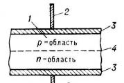
The power transformer T5 has three secondary windings, each of which has an output from the midpoint.
The IV winding provides the output voltage of +5 V. The SD2 diode assembly (semi-edible) forms with a winding of the IV bipoperiodic impact circuit with an average point (the average point of the IV winding point is grounded).
The SD2 assembly diodes are diodes with the Schottky barrier than the necessary speed is achieved and the efficiency of the rectifier is increased.
Winding III in conjunction with winding IV provides the output voltage of +12 in along with a diode assembly (semi-mounted) SD1. This assembly forms with a winding of the III bipoperiodic straightening scheme with an average point. However, the average point of the winding III is not grounded, but is connected to the output voltage bus +5 V. This will give the opportunity to use Schottki diodes in the channel of production +12 V, because The reverse voltage applied to the rectifier diodes with such an inclusion, decreases to the Schottky level allowed for diodes.
Elements L1, C6, C7 form a smoothing filter in the channel +12 V.
Resistors R9, R12 are designed to accelerate the discharge of the output capacitors of tires +5 V and +12 in after the UPS is turned off from the network.
Winding II with five removal provides a negative output voltage -5 V and -12 V.
Two discrete diodes D3, D4 form a two-fiber rectifier semicircle in the channel of production -12 B, and d5, d6 diodes - in channel -5 V.
Elements L3, C14 and L2, C12 form smoothing filters for these channels.
Winding II, as well as the winding III, is inserted by the reassuring RC chain R13, C13.
The average point of the winding II is grounded.
Stabilization of output voltages are carried out in different ways in different channels.
Negative output voltages -5 V and -12 in stabilize using linear integral three-water stabilizers U4 (type 7905) and U2 (type 7912).
To do this, the inputs of these stabilizers serves output voltages of rectifiers with C14 capacitors, C15. On the weekend capacitors C16, C17, stabilized output voltages are obtained -12 V and -5 V.
D7, D9 diodes provide the discharge of the output capacitors C16, C17 through resistors R14, R15 after turning off the UPS from the network. Otherwise, these capacitors would discharge through the scheme of stabilizers, which is undesirable.
Through resistors R14, R15, C14, C15 condensers are discharged.
D5, D10 diodes perform a protective function in case of breakdown of rectifying diodes.
If at least one of these diodes (D3, D4, D5 or D6) will be "punched", then in the absence of d5, d10 to the input of the integral stabilizer U1 (or U2) would be applied a positive pulse voltage, and through electrolytic capacitors C14 or C15 A variable current would occur, which would lead to their failure.
The presence of D5, D10 diodes in this case eliminates the possibility of such a situation, because The current closes through them.
For example, if the "breaks" diode D3, the positive part of the period, when D3 must be closed, the current will be closed on the chain: K-A D3 - L3 D7-D5- "Case".
Stabilization of the output voltage +5 V is carried out by the PWM method. To do this, a measuring resistive divider R51, R52 is connected to the output voltage bus. The signal proportional to the output voltage in the +5 V channel is removed from the R51 resistor and is fed to the inverting input of the DA3 error amplifier (output 1 of the control chip). On the direct input of this amplifier (output 2) fed by the reference voltage level, removed from the R48 resistor, which is included in the VR1, R49, R48 divider, which is connected to the output of the inner reference source of the U4 uref \u003d + 5 V. with changes in the voltage level of the tire + 5 B under the influence of various destabilizing factors, a change in the magnitude of mismatch (errors) between the reference and controlled voltage levels at the inputs of the DA3 error amplifier is changed. As a result, the width (duration) of the control pulses at the conclusions 8 and 11 of the U4 chip changes in such a way as to return the rejected output voltage +5 to the nominal value (with a decrease in the voltage on the tire +5 in the width of the control pulses increase, and with an increase in this voltage - decreases).
Output voltage +12 V in this UPS does not stabilize.
Adjusting the output voltage level This UPS is performed only for channels +5 V and +12 V. This adjustment is carried out by changing the level of reference voltage at the direct input of the DA3 error amplifier with the help of a VR1 trimmed resistor.
When the position of the VR1 engine is changed, during the UPS setting, the voltage level on the bus is +5 V, which means the +12 V bus, because Tire voltage +5 B is supplied to the middle point of the winding III.
Combined sewn of this UPS includes:
- limiting control circuit control pulse width;
- incomplete control of the output overvoltage (only on the +5 V bus).
Consider each of these schemes.
Limiting control circuit uses the T4 current transformer as a sensor, the primary winding of which is enabled sequentially with the primary winding of the power pulse transformer T5.
The R42 resistor is the load of the secondary winding T4, and D20, D21 diodes form a two-speech diagram of straightening the alternate pulse voltage removed from the load R42.
Resistors R59, R51 form a divider. Part of the voltage is smoothed by the C25 capacitor. The voltage level on this condenser proportionally depends on the width of the control pulses on the bases of the power transistors Q1, Q2. This level via the R44 resistor is supplied to the inverting input of the DA4 error amplifier (output 15 U4 chip). Direct input of this amplifier (output 16) grounded. D20, D21 diodes are included in such a way that the C25 capacitor when current flows through these diodes is charged to a negative (relative to the total wire) of the voltage.
In normal operation, when the width of the control pulses does not go out for the permissible limits, the output potential 15 is positive, due to the connection of this output through the R45 resistor with the UREF bus. With an excessive increase in the width of control pulses for any reason, the negative voltage on the C25 condenser increases, and the output potential 15 becomes negative. This leads to the appearance of the output voltage of the DA4 error amplifier, which before that was 0 B. Further increase in the width of the control pulses leads to the fact that the DA2 PWM-comparator shifts is transmitted to the DA4 amplifier, and the subsequent increase in the width of control pulses no longer occurs (restriction mode), because The width of these pulses ceases to depend on the feedback signal level on the direct input of the DA3 error amplifier.
The protection circuit from the KZ in loads can be conditionally divided into protection of the channels for the production of positive stresses and the protection of channels for the development of negative stresses, which are scheduled for approximately the same.
The sensor of the protection circuit from the KZ in the loads of the positive stress production channels (+5 V and +12 V) is a diode-resistive divider D11, R17, connected between the output tires of these channels. The voltage level on the anode diode D11 is a controlled signal. In normal mode of operation, when the voltages on the output tires of the channels +5 V and +12 V are nominal values, the potential of the diodine diodine D11 is about +5.8 V, because Through the divider-sensor flows from the tire +12 to the bus +5 in the chain: tire +12 V - R17-D11 - Tire +5 V.
The controlled signal from the anode D11 is fed to the resistive divider R18, R19. Some of this voltage is removed from the R19 resistor and is fed to the direct input of the comparator 1 of the U3 type LM339N chip. The inverting input of this comparator is supplied to the reference voltage level from the R27 resistor R26, R27 connected to the output of the uref \u003d + 5 reference source in the U4 control chip. The reference level is selected so that with normal operation mode, the potential of the direct input of the comparator 1 would exceed the potential of the inverse input. Then the output transistor of the comparator 1 is closed, and the UPS scheme is normally functioning in PWM mode.
In the case of a KZ in the load of the channel +12 in, for example, the potential of the diodine diode D11 becomes equal to O in, so the potential of the inverting input of the comparator 1 will become higher than the potential of the direct input, and the output transistor of the comparator will open. This will cause the closing of the transistor Q4, which is normally opened by a current base flowing through the chain: Upom bus - R39 - R36 B-E Q4 - "Case".
Opening the output transistor of the comparator 1 connects the R39 resistor to the "body", and therefore the Q4 transistor is passively closed by zero offset. Closing the transistor Q4 entails charging C22 condenser, which performs the function of the protection delay link. The delay is necessary from those considerations that in the process of the UPS output on the mode, the output voltages on the tires +5 V and +12 in appear not immediately, but as the output capacitors of the high capacity are charging. The reference voltage from the UREF source, on the contrary, appears almost immediately after turning on the UPS to the network. Therefore, in the start-up, the comparator 1 switches, its output transistor opens, and if there was no delaying capacitor C22, it would lead to the triggering of protection immediately when the UPS is turned on to the network. However, the C22 is included in the scheme, and the triggering of protection occurs only after the voltage on it reaches the level determined by the R37 resistor rates, the divisor connected to the UPOM bus and being the base for the transistor Q5. When this happens, the transistor Q5 opens, and the resistor R30 turns out to be connected through the small internal resistance of this transistor to the "case". Therefore, a way to flow the current of the base of the transistor Q6 by chain is appearing: uref - e-b Q6 - R30 - K-E Q5 "Case".
The transistor Q6 opens with this current to saturation, as a result of which the voltage uref \u003d 5 V, which is subtracted by the emitter, the transistor Q6 is applied through its small internal resistance to the output 4 of the U4 control microcircuit. This, as shown earlier, leads to the stopping of the digital microcircuit path, the disappearance of the output control pulses and the termination of the switching transistors Q1, Q2, i.e. To protective disconnection. The KZ in the load of the channel +5 V will lead to the fact that the potential of the diodine diodine D11 will be only about +0.8 V. Therefore, the output transistor of the comparator (1) will be open, and a protective shutdown will occur.
Similarly, a protection from the KZ in the loads of the negative stresses of the negative stresses (-5 V and -12 V) on the comparator 2 of the U3 chip is built. Elements D12, R20 form a diode-sized divider sensor, connected between the output tires of channels of negative stresses. The controlled signal is the potential of the diode diode cathode. When the CW in the load of the channel -5 B or -12 B, the potential of the cathode D12 increases (from -5.8 to 0 V to the CW in the load of the channel -12 V and to -0.8 V to the CZ in the load of the channel -5 B) . In any of these cases, a normally closed output transistor comparator 2 is opened, which causes the triggering of protection according to the above mechanism. In this case, the support level from the R27 resistor is supplied to the direct input of the comparator 2, and the potential of the inverting input is determined by the R22 resistors rates, R21. These resistors form a bipolarly populated divider (the R22 resistor is connected to the UREF \u003d + 5 V bus, and the R21 resistor to the diode cathode D12, the potential of which in the normal operation of the UPS, as already noted, is -5.8 V). Therefore, the potential of the inverting logger of the comparator 2 in the normal mode of operation is supported by smaller than the potential of the direct input, and the output transistor of the comparator will be closed.
Protection against output overvoltage on the +5 bus is implemented on ZD1, D19, R38, C23 elements. Stabilitron ZD1 (with a punching voltage of 5.1 V) is connected to the output voltage bus +5 V. Therefore, while the voltage on this bus exceeds +5.1 V, the stabilion is closed, and the transistor Q5 is closed. In case of increasing the voltage on the bus +5 above +5.1 V stabilitron "breaks through", and an unlocking current flows into the base of the transistor Q5, which leads to the opening of the transistor Q6 and the appearance of the UREF \u003d + 5 V voltage at the output 4 of the U4 control microcircuit, those. To protective disconnection. The R38 resistor is ballast for ZD1 stabitron. Capacitor C23 prevents the protection of protection in case of random short-term voltage emissions on the +5 V bus (for example, as a result of the voltage setting after a jump-shaking reduction of the load current). Diode D19 is unleashing.
The PG signal formation scheme in this UPS is a two-function and assembled on comparators (3) and (4) U3 microcircuits and a transistor Q3.
The scheme is constructed on the principle of controlling the presence of alternating low-frequency voltage on the secondary winding of the T1 starting transformer, which acts on this winding only in the presence of supply voltage on the primary winding T1, i.e. While the UPS is enabled in the feed network.
Almost immediately after turning on the UPS, the UPOM auxiliary voltage appears on the C30 capacitor, which is powered by the U4 control microcircuit and the U3 auxiliary microcircuit. In addition, the alternating voltage from the secondary winding of the T1 start transformer through the diode D13 and the current-limiting resistor R23 charges the C19 capacitor. With voltage with C19, the resistive divider R24, R25 is powered. From the R25 resistor, part of this voltage is fed to the direct input of the comparator 3, which leads to the closure of its output transistor. Appearing immediately following this, the output voltage of the internal support source of the U4 UREF \u003d + 5 chip in powers the R26, R27 divider. Therefore, a support level from the R27 resistor is supplied to the inverting input of the comparator 3. However, this level is selected smaller than the level of direct input, and therefore the output transistor of the comparator 3 remains in the closed state. Therefore, the process of charging the delayed capacity of C20 by chain begins: UPOM - R39 - R30 - C20 - "Case".
Growing as charging capacitor C20 The voltage is fed to the inverse input 4 of the U3 chips. On direct input of this comparator, voltage from the R32 R32 resistor R31, R32 connected to the UPOM bus is fed. While the voltage on the charging capacitor C20 does not exceed the voltage on the R32 resistor, the output transistor of the comparator 4 is closed. Therefore, the transistor base Q3 flows the opening current according to the chain: UPOM - R33 - R34 - B-E Q3 - "Corpus".
The transistor Q3 is open to saturation, and the PG signal, removed from its collector, has a passive low level and prohibits the start of the processor. During this time, during which the level of voltage on the C20 condenser reaches the level on the R32 resistor, the UPS has time to reliably exit the nomapsy mode of operation, i.e. All its output voltages appear in full.
As soon as the C20 voltage exceeds the voltage removed from R32, the comparator 4 will switch, and its output transistor will open. This entails the closing of the transistor Q3, and the PG signal, removed from its collector load R35, becomes active (n-level) and allows the start of the processor.
When the UPS is turned off from the network on the secondary winding of the T1 start transformer, the alternating voltage disappears. Therefore, the voltage on the C19 condenser is rapidly reduced due to the low capacity of the latter (1MKF).
As soon as the voltage drop on the R25 resistor will become less than on the R27 resistor, the comparator 3 switches, and its output transistor will open. This will entail a protective disconnection of the output voltages of the U4 control chip, because The transistor Q4 opens. In addition, through an open output transistor of the comparator 3, the process of accelerated discharge of the C20 condenser will begin: (+) C20 - R61 - D14 - K-E output transistor of the comparator 3 - "Case". As soon as the voltage level on C20 becomes smaller than the voltage level on R32, the comparator 4 will switch, and its output transistor closes. This will entail the Opening of the transistor Q3 and the transition of the PG signal into an inactive low level before it is unacceptable to decrease the voltage at the UPS output tires. This will lead to the initialization of the computer reset signal and to the initial state of the entire digital part of the computer.
Both comparators 3 and 4 schemes for generating a PG signal are covered by positive feedback using R28 and R60 resistors, respectively, which speeds up their switching.
Smooth output to the mode in this UPS is traditionally provided by the forming chain C24, R41 connected to the output 4 of the U4 control chip. The residual voltage at the output 4, which determines the maximum possible duration of the output pulses, is given by the divider R49, R41.
The fan motor power is carried out by voltage from the C14 condenser in the voltage generation channel -12 v via an additional unleashing M-shaped filter R16, C15.